OSH Park
XC9536 Breakout Board
- You need to sign in or sign up before continuing.
XC9536 Breakout Board
by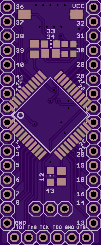
2
layer board of
0.70x1.70
inches
(17.78x43.18
mm).
Shared on
September 13th, 2013 21:50.
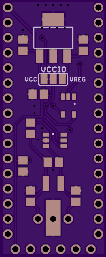
DIP-32 Breakout Board for XC9536(XL) with 30 GPIO’s, 1 crystal oscillator, 2 LED’s, a debounced tactile switch as GCLR, and on-board voltage regulator for separate VCCIO (defaults to VCCIO = VCC)
Component list
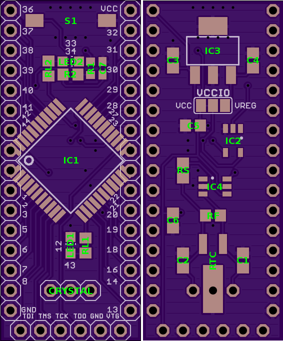
IC1: Xilinx XC9536 or XC9536XL[1]
IC2: TI SN74LVC1G17DBV (SOT-23) single Schmitt-trigger buffer (non-inverting)
IC3: Fixed voltage regulator (SOT-223) [2]
IC4: TI SN74LVC1GX04 crystal oscillator driver[3]
S1: Tyco Electronics FSMSM momentary tactile switch
LED1/LED2: 0805 chip LED
R1: 0603 SMD resistor, 82Kohm
R2: 0805 SMD resistor, 18Kohm
RL1/RL2: 0805 SMD resistors, 330ohm
RF/RS: 0805 SMD resistor[3]
C1/C2: 0805 SMD capacitors [3]
C3/C4: 0805 SMD capacitors [2]
C5/C6: 0805 SMD capacitor, 100nF
C7: 0603 SMD capacitor, 1uF
Crystal: HC-49 crystal/resonator[3]
RTC: 32.768KHz crystal[3]
[1] This board supports both the XC9536 and XC9536XL CPLD’s from Xilinx. These chips are nearly identical, except for the fact that the XL chip is a 3V part, and the non-XL chip is a 5V part. However, the XL chip does have 5V-tolerant I/O pins, and the non-XL chip is obsolete. The chip used will affect the voltage of the VCCIO regulator.
[2] Fixed voltage regulator, in SOT-223 package. The Microchip MCP1826S is a good choice. For the XC9536, a 3.3V or 1.8V regulator can be used, depending on the IO logic level you wish to use. For the XC9536XL, use a 1.8V regulator. Once a regulator has been selected, refer to the datasheet for C3 (input) and C4 (output) values. The board defaults to VCCIO = VCC. If you want to use the regulator as the I/O reference voltage, you must cut the trace between the VCC and VCCIO jumpers, then connect the VREG and VCCIO jumpers (marked on the bottom of the board).
[3] There are footprints on the board to support either a standard HC-49 crystal or resonator, or a 32.768KHz RTC. If a resonator with internal capacitors is used, C1 and C2 can be omitted. Otherwise, C1 and C2 can be calculated from the crystal’s specified load capacitance using the formula C1 = C2 = 2(CL + CS) where CL is the crystal’s rated load capacitance and CS is the IC’s stray capacitance (5pF for the SN74LVC1GX04DBVR). Do not use CL for C1/C2. RF is the oscillator’s biasing feedback resistor, and should be between 1Mohm and 10Mohm. RS should be selected such that its restance is equal to the reactance of C2 at the oscillating frequency.