OSH Park
Electronic clock switch for 1Chip-SNES, SNES Mini and Jr.
- You need to sign in or sign up before continuing.
Electronic clock switch for 1Chip-SNES, SNES Mini and Jr.
by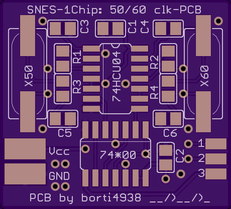
2
layer board of
1.15x1.04
inches
(29.24x26.52
mm).
Shared on
January 7th, 2015 19:04.
Solder Joints:
1 - mode (in) Vcc = PAL-mode, GND = NTSC-mode, same as at S-CPUN pin111
2 - inverted mode (out) to be jointed to lifted pin9 of S-RGB IC
3 - clock (out) to be jointed S-CPUN pin9 (either remove X1 or lift pin9 on S-CPUN)
Values of passive components (all 0805 packages except crystals):
R1, R2: 330Ohm
R3, R4: 1MOhm
C1, C2: 0.1uF
C3 - C6: 22pF (exact value: C3=C4=C5=C6= 2*(CL-CS), where CL is load cap. and CS is stray cap. of 74HCU04)
X50: 17.734MHz
X60: 21.477MHz
Active ICs (SOIC14 packages):
74*00: four 2-NAND gates, use 7400, 74LS00, 74HC00, and so on
74HCU04: six inverter, using unbuffered inverter as displayed performs best