
OSH Park
Profile for borti4938
Shared projects
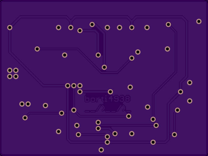
SNES multi region mod [now tested]
by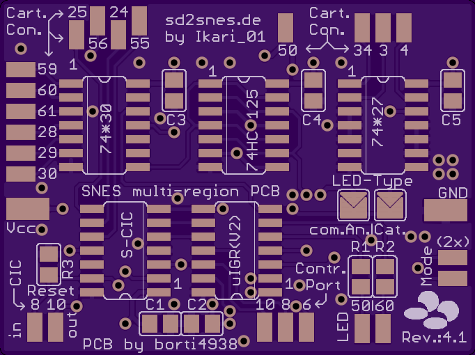
2
layer board of
1.71x1.28
inches
(43.36x32.41
mm).
Shared on
January 7th, 2015 19:10.
Includes SuperCIC, uIGR and Regionpatching. The part of regionpatching is new designed!
Solder Joints:
- Most of the solder joints are located at the cart connector as to be seen
on the silkscreen.
- The mode output located at the PCBs bottom right side is goin' to the
- S-CPUN Pin 111
- S-PPU1 Pin 24 and S-PPU2 Pin 30
- One may use the additional pad for the add-on PCB for the 1Chip-SNES or to use separate wires to S-PPU1 and S-PPU2
- CIC8 and CIC10 has to be solder to the pads, not the the lifted pins
- Reset input can be solder directly to the reset buttons output instead of CIC8
- ‘Contr. Port’ means the connector for the flat wire. In the SNES-mini the mapping is as follows:
- 10 -> Player1 Pin3
- 8 -> Player1 Pin2
- 6 -> Player1 Pin4
Lifted Pins:
- S-CPUN Pin 111 OR S-PPU1 Pin 24 and S-PPU2 Pin 30
- CIC Pins 1, 2, 10 and 11 OR remove CIC completely
Values of passive components:
R1, R2: 220Ohm (increase resistor values if LED is too bright)
R3: 10kOhm
C1 - C5: 0.1uF
Active ICs (SOIC14 packages):
74*27: three 3-NOR gates, where two are unused
74*30: 8-NAND gate
74HC(T)125: four buffer gate: use HC or HCT type!
S-CIC: PIC16F630 flashed with ‘Firmware_SCIC.hex’
uIGR (V2): PIC16F684 flashed with ‘Firmware_uIGR_V2.hex’
Both firmwares can be found at https://github.com/borti4938/SNES-AddOn-PCBs/tree/master/Firmware-Switchless-PICs
!!!Note that the ‘snes-igr.hex’ in the sd2snes github repository, i.e., the ‘classical igr’ won’t work
on this PCB!!!
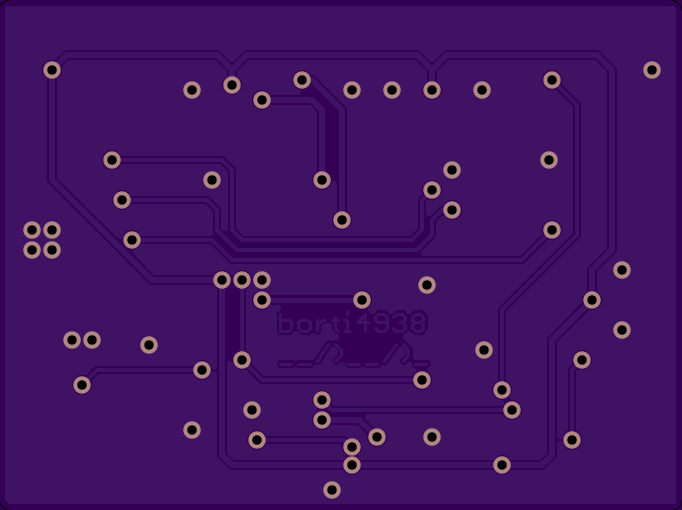
SNES multi region mod with SuperCIC, uIGR (V2) and region patching parts
by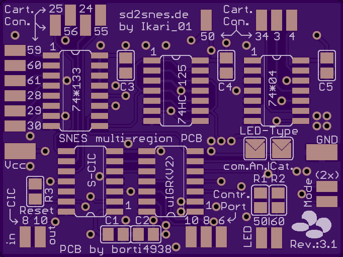
2
layer board of
1.71x1.28
inches
(43.36x32.41
mm).
Shared on
January 7th, 2015 19:10.
Solder Joints:
- Most of the solder joints are located at the cart connector as to be seen
on the silkscreen.
- The mode output located at the PCBs bottom right side is goin' to the
- S-CPUN Pin 111
- S-PPU1 Pin 24 and S-PPU2 Pin 30
- One may use the additional pad for the add-on PCB for the 1Chip-SNES or to use separate wires to S-PPU1 and S-PPU2
- CIC8 and CIC10 has to be solder to the pads, not the the lifted pins
- Reset input can be solder directly to the reset buttons output instead of CIC8
- ‘Contr. Port’ means the connector for the flat wire. In the SNES-mini the mapping is as follows:
- 10 -> Player1 Pin3
- 8 -> Player1 Pin2
- 6 -> Player1 Pin4
Lifted Pins:
- S-CPUN Pin 111 OR S-PPU1 Pin 24 and S-PPU2 Pin 30
- CIC Pins 1, 2, 10 and 11 OR remove CIC completely
Values of passive components:
R1, R2: 220Ohm (increase resistor values if LED is too bright)
R3: 10kOhm
C1 - C5: 0.1uF
Active ICs (SOIC14 packages if not otherwise stated):
7404: six inverter gates, where three are unused
74HC(T)125: four buffer gate: use HC or HCT type!
74133: 13-NAND gate, SOIC16 package
S-CIC: PIC16F630 flashed with ‘Firmware_SCIC.hex’
uIGR (V2): PIC16F684 flashed with ‘Firmware_uIGR_V2.hex’
Both firmwares can be found at https://github.com/borti4938/SNES-AddOn-PCBs/tree/master/Firmware-Switchless-PICs
!!!Note that the ‘snes-igr.hex’ in the sd2snes github repository, i.e., the ‘classical igr’ won’t work
on this PCB!!!
Electronic clock switch for 1Chip-SNES, SNES Mini and Jr.
by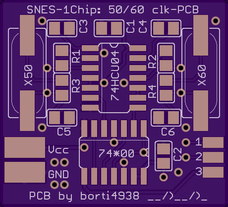
2
layer board of
1.15x1.04
inches
(29.24x26.52
mm).
Shared on
January 7th, 2015 19:04.
Solder Joints:
1 - mode (in) Vcc = PAL-mode, GND = NTSC-mode, same as at S-CPUN pin111
2 - inverted mode (out) to be jointed to lifted pin9 of S-RGB IC
3 - clock (out) to be jointed S-CPUN pin9 (either remove X1 or lift pin9 on S-CPUN)
Values of passive components (all 0805 packages except crystals):
R1, R2: 330Ohm
R3, R4: 1MOhm
C1, C2: 0.1uF
C3 - C6: 22pF (exact value: C3=C4=C5=C6= 2*(CL-CS), where CL is load cap. and CS is stray cap. of 74HCU04)
X50: 17.734MHz
X60: 21.477MHz
Active ICs (SOIC14 packages):
74*00: four 2-NAND gates, use 7400, 74LS00, 74HC00, and so on
74HCU04: six inverter, using unbuffered inverter as displayed performs best